A. Conolly, R. Ely, M. Garcia-Sciveres, C. Haber, M. Paulini, D. Ray, I. Volobuev, W. Yao.
An Introduction to SVXII
Run I of the Tevatron Collider at Fermilab ended on February 20, 1996, with a
total integrated luminosity recorded by the Collider Detector at Fermilab (CDF)
of roughly ![]() .
During this run, the vertex reconstruction capability of CDF
went from being in itself an experiment,
to becoming the heavy flavor detection method that made possible
the observation of the top quark and the measurement of its mass,
as well as a wealth of b physics previously untapped in
hadron colliders.
Vertexing in CDF began with the SVX detector, which was replaced
after
.
During this run, the vertex reconstruction capability of CDF
went from being in itself an experiment,
to becoming the heavy flavor detection method that made possible
the observation of the top quark and the measurement of its mass,
as well as a wealth of b physics previously untapped in
hadron colliders.
Vertexing in CDF began with the SVX detector, which was replaced
after ![]() with a radiation hard ``replica'', SVX'. For
Run II of the Tevatron (to begin in 1999), CDF will replace SVX' with
a new silicon detector, SVXII. Whereas SVX pioneered the use of a new
technology in collider detectors, SVXII will seek to push this
technology in several directions at once, so that while not as
obvious, the challenge is equally great.
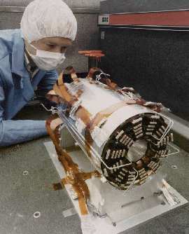
SVXII will use 720 double-sided, 7.43cm long silicon sensors
(width depends on layer), arranged in 5 coaxial cylinders (layers).
A readout unit will consist of two
sensors wire-bonded end-to-end with electronics on one of the sensors.
Readout units will be mechanically paired, end-to-end with the electronics
on the far ends, to form 29.8cm long ``ladders''.
Ladders will be held in 5-layer ``barrel'' structures with 12 ladders per
layer. Each barrel will have 2 beryllium bulkheads for mechanical support and
electronics cooling. There will be 3 barrels end-to-end for a combined
length of 87cm and a total of 405,504 readout channels.
The innovative
features of SVXII that people at LBNL work on are
(1) new ``deadtimeless'' electronics with fast digital readout
that will permit implementation of a secondary vertex trigger, and
(2) aggressive packaging to place the readout chips
directly on active detector surfaces.
with a radiation hard ``replica'', SVX'. For
Run II of the Tevatron (to begin in 1999), CDF will replace SVX' with
a new silicon detector, SVXII. Whereas SVX pioneered the use of a new
technology in collider detectors, SVXII will seek to push this
technology in several directions at once, so that while not as
obvious, the challenge is equally great.
SVXII will use 720 double-sided, 7.43cm long silicon sensors
(width depends on layer), arranged in 5 coaxial cylinders (layers).
A readout unit will consist of two
sensors wire-bonded end-to-end with electronics on one of the sensors.
Readout units will be mechanically paired, end-to-end with the electronics
on the far ends, to form 29.8cm long ``ladders''.
Ladders will be held in 5-layer ``barrel'' structures with 12 ladders per
layer. Each barrel will have 2 beryllium bulkheads for mechanical support and
electronics cooling. There will be 3 barrels end-to-end for a combined
length of 87cm and a total of 405,504 readout channels.
The innovative
features of SVXII that people at LBNL work on are
(1) new ``deadtimeless'' electronics with fast digital readout
that will permit implementation of a secondary vertex trigger, and
(2) aggressive packaging to place the readout chips
directly on active detector surfaces.
Table 1 compares some parameters of Run I relevant to
silicon detector operation with the goals for Run II. The Tevatron luminosity
will increase by more than an order of magnitude, primarily through the
addition of more circulating bunches.
The large number
of bunches means that there is no longer enough time between
successive crossings for any kind of trigger decision. For Run II,
therefore, all CDF detector elements must queue data from every beam crossing
into a pipeline, waiting for the trigger processor to catch up. A 5.5 ![]() sec
trigger latency means that SVXII must remember 42 beam crossings. But perhaps
the most ambitious aspect of the SVXII design is the desire to read out the
detector at a projected rate of 40kHz in order to use SVXII information
in a second level hardware trigger
The hope is to develop a hadronic b trigger based on
vertexing.
An application specific integrated circuit (ASIC) denominated svx3
will implement the necessary data pipeline and
accomodate the high readout rate without compromising livetime.
sec
trigger latency means that SVXII must remember 42 beam crossings. But perhaps
the most ambitious aspect of the SVXII design is the desire to read out the
detector at a projected rate of 40kHz in order to use SVXII information
in a second level hardware trigger
The hope is to develop a hadronic b trigger based on
vertexing.
An application specific integrated circuit (ASIC) denominated svx3
will implement the necessary data pipeline and
accomodate the high readout rate without compromising livetime.
In a hadron collider the interaction region is long
in the beam direction (![]() cm for CDF). This means that in
order to achieve high acceptance a vertex detector must be long.
However, the need for radiation hardness drives the active surface
area of each readout channel to be as small as possible.
Therefore, a strip detector must have short strips,
making it necessary to place readout electronics within the active volume.
In SVXII the electronics will be
directly on the sensor surface, in order to avoid acceptance gaps.
cm for CDF). This means that in
order to achieve high acceptance a vertex detector must be long.
However, the need for radiation hardness drives the active surface
area of each readout channel to be as small as possible.
Therefore, a strip detector must have short strips,
making it necessary to place readout electronics within the active volume.
In SVXII the electronics will be
directly on the sensor surface, in order to avoid acceptance gaps.
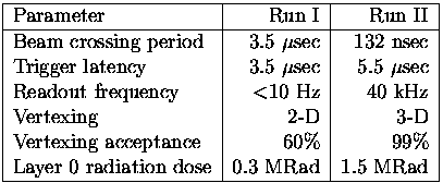
Table 1: Comparison of Run I and Run II selected silicon detector
parameters. The trigger latency refers to the lowest level
trigger. Readout frequency refers to how often the silicon
detector is fully read out.
Layer 0 is the silicon layer closest to the beam pipe.
The packages that will hold the svx3 ASICS on the sensor active surfaces
are called hybrids.
Hybrids provide power and signal distribution as well as heat dissipation.
Dead-timeless operation places many demands on the geometry of the
hybrid connections and on the location of components other than the
svx3 ASICs. But also related to geometry the thermal performance must be
adequate to keep the sensors below ![]() C. And to add even further
complication, because the electronics are
in the detector active volume the hybrid mass must be minimized
to prevent excessive multiple scattering.
C. And to add even further
complication, because the electronics are
in the detector active volume the hybrid mass must be minimized
to prevent excessive multiple scattering.
Excluding the hybrids, the
average material seen by a particle traversing the SVXII is estimated at
4.4% of a radiation length (RL). Hybrids will be fabricated of
printed thick film metal and dielectric on beryllium oxide ceramic
(BeO). The thick film process used a fired tape dielectric that permits
multiple layers with ![]() m traces and spaces, as well as vias on a
m traces and spaces, as well as vias on a
![]() m pitch. The process can combine gold traces with silver power and
ground planes to reduce mass.
These BeO hybrids will add another 4.4%RL to the SVXII average
material, which is deemed acceptable.
m pitch. The process can combine gold traces with silver power and
ground planes to reduce mass.
These BeO hybrids will add another 4.4%RL to the SVXII average
material, which is deemed acceptable.
This Figure
shows a schematic cross section of the electronics end of an SVXII
readout unit or half-ladder. Only one of the two sensors in the half-ladder
is represented (not to scale).
Hatched shapes are silicon, open shapes are hybrids, and cross
hatched is the bulkhead support/cooling channel. FE chips are marked 1,
BE chips 2, readout cable 3, bulkhead 4, sensor 5,
jumper 6, and jumper wire-bonds 7.
The need to read out both sides of the sensor, as well as to support and cool
the ladder forces the chips on the bottom (side view) far from the sensor end.
This impacts on cooling, demanding a substrate thickness that
increases rapidly with hybrid length. Given a power dissipation of 450mW per
svx3 chip (derived from measurements on prototypes) and a reasonably
achievable coolant temperature of ![]() C at the ladder, a BeO
substrate thickness of 500
C at the ladder, a BeO
substrate thickness of 500![]() m is required for a maximum sensor
temperature of
m is required for a maximum sensor
temperature of ![]() C at the ladder mid-point after a 1.5MRad
dose.
C at the ladder mid-point after a 1.5MRad
dose.
Another challenge of placing readout hybrids on both sides of the sensor is
making electrical connections to the bottom hybrid. A separate cable is
mechanically not feasible without increasing layer radii, as well as
electrically problematic because both hybrids read the same sensor, which
favors tying them into a compact circuit. A conventional
flex cable connecting the top and bottom hybrids is not possible because
side-by-side ladders in the same layer must be very close to produce
overlapping strips essential for off-line internal alignment (typical gaps
are of order 2mm). The solution developed at LBNL (using the UC Berkeley
Microlab) uses a very small
(1.8mm ![]() 1.5mm
1.5mm ![]() 0.6mm) L-shaped jumper glued to the
edge of the sensor
(see end view of figure 2) that has
0.6mm) L-shaped jumper glued to the
edge of the sensor
(see end view of figure 2) that has ![]() m diameter vias routing all
connections from bonding pads on the top to pads on the bottom. Hybrids have
a field of pads on one side for wire-bonding to the jumper.
m diameter vias routing all
connections from bonding pads on the top to pads on the bottom. Hybrids have
a field of pads on one side for wire-bonding to the jumper. ![]() m
traces are used to scramble the connections on the jumper so that identical
hybrids can be used on both sides of the sensor. The jumper is made out of
laser-drilled alumina ceramic plus a combination of thick-film metalization
to produce the vias and thin film integrated circuit methods for the fine
features on the top and bottom surfaces.
m
traces are used to scramble the connections on the jumper so that identical
hybrids can be used on both sides of the sensor. The jumper is made out of
laser-drilled alumina ceramic plus a combination of thick-film metalization
to produce the vias and thin film integrated circuit methods for the fine
features on the top and bottom surfaces.